Plowing-induced nanoexfoliation of mono- and multilayer MoS₂ surfaces
New article in journal "Physical Review Materials"
Published:
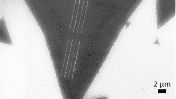
The surface structures resulting from scratching monolayer MoS2 on SiO2 and multilayer MoS2 using diamond nanotips with normal forces up to 3µN and scan velocities up to 10µm/s in ambient conditions are compared. In both cases the damage process initiates with normal forces of about 2µN. As shown by postmortem AFM images the monolayer is peeled off along the zigzag direction of MoS2 and folded in the form of flat triangular flakes. Wrinkling and multiple folding can be associated to debris accumulation originated from the SiO2 substrate, which is also scratched by the tip. On the multilayer MoS2 thicker chips with linear size of about 100 nm and height of few tens of nm are rolled out. The chipping is associated to a distinct stick-slip motion of the AFM tip with repetition period logarithmically increasing with the velocity but definitely below the chip length, suggesting that the process occurs through a series of exfoliation events. Simple energetic considerations allow to explain why peeled monolayers tend to fold over the untreated surface while thicker layers tend to bend and form chips.
Alper Özogul, Felix Trillitzsch, Christof Neumann, Antony George, Andrey Turchanin, Enrico Gnecco: "Plowing-induced nanoexfoliation of mono- and multilayer MoS2 surfaces", Phys. Rev. Materials 4 (2020) 033603, DOI: 10.1103/PhysRevMaterials.4.033603External link